
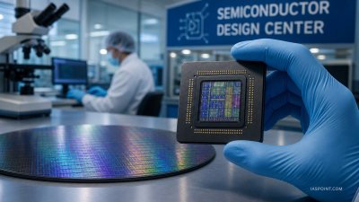
NIELIT has released the Semiconductor Laboratory (SCL) indigenous 1.2‑micrometre Process Design Kit (PDK) on the MeitY-funded eChipHub platform for integrated‑circuit design, prototyping and semiconductor education.
Key features of the PDK
- Process node: 1.2 µm CMOS technology for analog and digital design flows.
- Contents: technology files, design rules, device models and layout‑versus‑schematic (LVS) parameters required for fabrication‑matched design.
- Toolchain compatibility: packaged for use with open‑source Electronic Design Automation (EDA) toolchains.
- Use cases: prototype chips, academic labs, curriculum integration and MSME/startup product development.
Access and platform
- Distribution channel: available through eChipHub, managed by NIELIT and developed with SoCTeamup Semiconductors Pvt Ltd.
- Authentication: secure Aadhaar‑authenticated download mechanism on eChipHub.
- Eligibility: access model targets students, researchers, teachers, startups, MSMEs and industry professionals.
Training and ecosystem linkages
- Capacity building: linked programmes include courses, bootcamps, internships and faculty development; ~30,000 students expected to benefit.
- Institutional link: SCL Mohali provides the fabrication/process expertise behind the PDK.
- Policy linkage: the release is linked to the India Semiconductor Mission ecosystem initiatives.
IASPOINT Booster Facts
- NIELIT: functions under the Ministry of Electronics and Information Technology (MeitY).
- CMOS: Complementary Metal‑Oxide‑Semiconductor.
- PDK role: essential for design‑to‑foundry compatibility and verification before tape‑out.