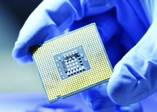
India has expanded its semiconductor talent development push under the Chips to Startups (C2S) initiative of the India Semiconductor Mission. The programme aims to build a skilled workforce for chip design, fabrication, packaging and testing. It also supports India’s wider goal of strengthening self-reliance in the semiconductor sector.
Training Push Under C2S
The initiative focuses on training 85,000 engineers in semiconductor design over a 10-year period. India has already made notable progress in the first four years of the programme. The effort is designed to create a steady pipeline of skilled professionals for the fast-growing chip industry.
Open-Access EDA Tools in Colleges
World-class Electronic Design Automation (EDA) tools from major global firms have been made available in 315 academic institutions across India. These tools allow students to gain practical experience in semiconductor chip design. The chips designed by students are then fabricated and tested at the Semiconductor Laboratory in Mohali, giving them exposure to the full chip development cycle.
Scale and Industry Relevance
The programme has become the world’s largest open-access EDA initiative. More than 1.85 crore hours of EDA tool usage have been recorded so far. Students from across the country, from Assam to Gujarat and from Kashmir to Kanyakumari, are participating in semiconductor design activities. This reflects growing national capacity in a strategic technology sector.
Expansion Under ISM 2.0
Under India Semiconductor Mission 2.0, the programme will be expanded from 315 to 500 academic institutions. The move is intended to widen access to semiconductor training and build a larger talent base. The global semiconductor industry is expected to grow from USD 800–900 billion to USD 2 trillion, creating demand for nearly 2 million skilled professionals.
Last Modified: April 28, 2026