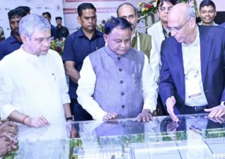
The foundation stone for India’s first advanced 3D chip packaging unit was laid on 19-20 April 2026 at Info Valley, Bhubaneswar, Odisha. The project is implemented by US-based 3D Glass Solutions Inc. through its Indian subsidiary, Heterogeneous Integration Packaging Solutions Pvt Ltd (HIPSPL). It received approval under the India Semiconductor Mission (ISM) in 2025.
Project Investment and Capacity
The unit involves an investment of approximately ₹1,943 crore. It will specialise in advanced 3D glass substrate packaging technology, using specialised glass substrates for three-dimensional integration of electrical components. The plant aims to produce 70,000 glass panels annually, 50 million assembled units, and 13,000 advanced 3D heterogeneous integration (3DHI) modules.
Timeline and Employment
Commercial production is targeted to begin by August 2028, with full-scale capacity utilisation expected by August 2030. The project is expected to generate around 2,500 direct and indirect jobs.
Strategic Importance and Applications
The unit is designed for applications in artificial intelligence (AI), 5G/6G communications, defence systems, data centres, and high-performance computing. It aims to reduce India’s dependence on imported chip packaging technology.
Odisha’s Semiconductor Industry Status
Odisha is the first Indian state to host both a compound semiconductor fabrication unit by SiCSem Private Limited and an advanced glass substrate-based packaging unit. The India Semiconductor Mission was launched to promote semiconductor manufacturing and design in India. Advanced 3D chip packaging enhances performance by integrating multiple layers of semiconductor devices.
Last Modified: April 20, 2026