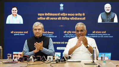
Rajasthan entered the high-technology manufacturing sector with the inauguration of its first semiconductor manufacturing cluster on May 15, 2026, at Bhiwadi in the Alwar district. The facility marks India’s first Small and Medium Enterprise (SME) led semiconductor chip Assembly, Testing, Marking, and Packaging (ATMP) and Outsourced Semiconductor Assembly and Test (OSAT) unit. Virtually inaugurated by Union Electronics and IT Minister Ashwini Vaishnaw and Rajasthan Chief Minister Bhajan Lal Sharma, the launch coincided with the operationalization of the Rajasthan Semiconductor Policy of March 2026. This initiative establishes the state as a key participant in the global electronics value chain and strengthens the industrial belt connected to the Delhi-National Capital Region (NCR).
Infrastructure and Financial Investment
The semiconductor unit is established by Sahasra Semiconductors Private Limited within the greenfield Electronics Manufacturing Cluster (EMC) located at Salarpur, Khushkhera in Bhiwadi.
Capital Expenditure and Scaling
- Sahasra Plant Investment: Developed with a capital outlay exceeding Rs 150 crore.
- Fiscal Support: The plant received financial incentives under the central Scheme for Promotion of Manufacturing of Electronic Components and Semiconductors (SPECS), managed by the Ministry of Electronics and Information Technology (MeitY).
- Industrial Cluster Investment: The overarching EMC, developed by ELCINA Electronics Manufacturing Cluster Private Limited, has attracted total investment commitments exceeding Rs 1,200 crore from 20 participating companies.
- Operational Progress: Eleven companies have already commenced commercial production inside the cluster, representing a combined investment of approximately Rs 900 crore.
Plant Infrastructure and Cleanrooms
The Sahasra packaging facility spans an area of 57,000 square feet. It is equipped with controlled environments categorized into Class 10K and Class 100K cleanrooms. These specifications regulate the maximum allowable particle count per cubic foot of air, providing the required baseline environment for downstream semiconductor packaging, final testing, and automated micro-assembly operations.
Production Capabilities and Export Orientation
The plant focuses on the backend stage of the semiconductor supply chain, converting fabricated silicon wafers into completed commercial components.
Target Product Portfolio
The Bhiwadi facility manufactures and packages five primary categories of micro-electronic devices:
- Memory Modules: Chips tailored for Micro Secure Digital (microSD) cards and heavy-duty flash storage units.
- Telecommunication Modules: Embedded Subscriber Identity Modules (eSIMs) for cellular and IoT connectivity.
- Power Management Devices: Integrated Circuits (ICs) designed specifically as LED drivers.
- Tracking Hardware: Radio Frequency Identification (RFID) products used in automation and logistics.
- Advanced Storage Solutions: Solid State Drives (SSDs) and Dynamic Random-Access Memory (DRAM) architectures.
Capacity Scaling and Market Distribution
| Metric | Current Status (2026) | Target Status (Within 2–3 Years) |
| Annual Packaging Volume | 60 million semiconductor units | 400 million to 600 million units |
| Primary Economic Focus | Domestic and Global Markets | Expansion into advanced packaging R&D |
| Export Share | Over 60% of total production | Scaling global supply network |
The facility currently exports the majority of its microchips to international destinations, including the United States, Germany, France, Eastern European nations, China, and Nepal.
Rajasthan Semiconductor Policy 2026
The launch of the Bhiwadi cluster aligns with the guidelines outlined in the Rajasthan Semiconductor Policy released in March 2026. The policy aims to move the state’s economic profile from traditional industries toward tech-driven high-end manufacturing.
Key Incentives Offered
- Fiscal Subsidies: Provision of up to 60% capital subsidy for projects approved under the India Semiconductor Mission (ISM), alongside a 5% interest subsidy on commercial term loans.
- Utility and Duty Waivers: A 100% exemption from state electricity duty for a fixed tenure of seven years from the commencement of operations.
- Land and Transaction Benefits: A 75% rebate on official stamp duty and mandatory land conversion charges.
- Environmental Support: Up to 50% reimbursement for expenses incurred on green rating compliance and environmentally sustainable infrastructure.
Dedicated Semiconductor Corridors
To streamline clearances and ensure resources reach manufacturing units, the state government is establishing dedicated industrial zones. These include the Jodhpur-Pali-Marwar industrial belt and the Kankani Industrial Area. These regions feature fast-track land allocation, single-window statutory clearances, and guaranteed uninterrupted power and water supply lines.
Socio-Economic and Skill Impacts
The operationalization of the current semiconductor units has generated direct employment for approximately 2,500 to 2,700 personnel. Expected future expansions will generate technical openings in specialized domains, including electronics engineering, chip architecture design, robotic automation, artificial intelligence deployment, and high-tech assembly quality control. To bridge the technical talent gap, the plant functions alongside the Electronics Sector Skills Council of India (ESSCI) and state-run technical institutes to train regional youth in advanced chip packaging and machine automation methodologies.
IASPOINT Booster Facts for UPSC
- ATMP vs. Fabrication: Wafer Fabrication is the front-end process where circuitry is etched onto silicon wafers in Class 10 or Class 100 cleanrooms. ATMP/OSAT is the back-end process involving cutting, wire bonding, testing, and housing the chips into protective casings.
- SPECS Scheme: Launched by MeitY, the Scheme for Promotion of Manufacturing of Electronic Components and Semiconductors provides a financial incentive of 25% on capital expenditure for selected electronic goods and component supply chains.
- EMC Scheme: The Electronics Manufacturing Clusters scheme provides grant assistance for setting up shared world-class infrastructure, testing centers, and logistics hubs for electronics factories.
- India Semiconductor Mission (ISM) 2.0: The Union Budget 2026–27 allocated Rs 1,000 crore for ISM 2.0 to support industry-led research, dedicated semiconductor workforce training, and specialized packaging ecosystems.
- Cleanroom Standards: A Class 10K cleanroom allows no more than 10,000 particles of size 0.5 microns or larger per cubic foot of air, whereas advanced fabrication plants require Class 1 or Class 10 standards.
- Geographical Advantage: Bhiwadi lies directly within the influence zone of the Delhi-Mumbai Industrial Corridor (DMIC) and benefits from close proximity to the Western Dedicated Freight Corridor (WDFC), facilitating rapid logistics.