
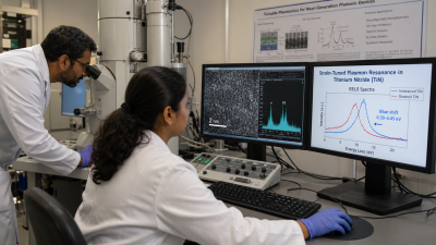
On 7 July 2026, JNCASR researchers reported that applying mechanical strain to epitaxial ultrathin titanium nitride (TiN) films shifts their plasmon resonance, enabling active tuning of metal optical response.
Key experimental findings
- Blue shift: Strained TiN films exhibit a plasmon resonance blue shift of 0.30–0.45 eV versus unstrained films.
- Mode behaviour: Both screened and unscreened plasmon modes shift consistently with local strain distribution.
- Plasma frequency: Increase tracked to a higher free-electron concentration in strained regions.
Material and microscopic mechanism
- Titanium nitride (TiN): CMOS-compatible, gold-like plasmonic response with high thermal and chemical stability.
- Nitrogen vacancies: DFT shows tensile strain lowers formation energy of N vacancies; vacancies act as electron donors, raising carrier density.
Techniques and sample design
- Probes used: Electron energy loss spectroscopy (near-atomic resolution), spectroscopic ellipsometry, high-resolution X-ray diffraction, and DFT calculations.
- Samples: Two 10 nm epitaxial films — strain-free on MgO and tensile-strained via an Al0.3Sc0.7N buffer layer.
Applications and relevance
- Reconfigurable nanophotonics: Strain control allows on-chip active tuning of plasmonic resonances for modulators and tunable metasurfaces.
- Potential domains: Optical sensors, on-chip interconnects for AI data centres, and components for quantum photonic networks.
IASPOINT Booster Facts
- Plasma frequency formula: ωp = sqrt(ne^2/ε0 m*); increases with free-electron density n.
- EELS: Directly measures plasmon energy loss; spatially maps local plasmon shifts.
- CMOS compatibility: Enables integration of plasmonic elements with silicon photonics.
- DFT role: Predicts vacancy formation energies and electronic structure changes under strain.