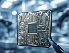
India is strengthening its semiconductor ecosystem through the Chips to Start-up (C2S) Programme, a capacity-building initiative aimed at developing chip design talent, supporting startups, and expanding access to advanced design infrastructure. The programme is part of a wider effort to position India as a key contributor to the global semiconductor value chain.
Programme Objective
The C2S Programme was launched by the Ministry of Electronics and Information Technology in 2022 with a total outlay of ₹250 crore over five years. It seeks to build an industry-ready semiconductor workforce and support indigenous innovation in chip design. The programme covers academic institutions, researchers, students, and startups across the country.
Scale and Coverage
The initiative currently spans around 400 organisations, including 305 academic institutions and 95 startups. It aims to develop 85,000 industry-ready professionals through undergraduate, postgraduate, and doctoral training. The target includes:
- 200 PhD scholars in advanced chip design research.
- 7,000 M.Tech graduates in VLSI or Embedded Systems.
- 8,800 M.Tech graduates with VLSI exposure.
- 69,000 B.Tech students trained in VLSI-oriented coursework.
Infrastructure and Implementation
The programme provides access to shared EDA tools, SMART labs, high-performance computing, and fabrication support. The ChipIN Centre at C-DAC Bengaluru acts as a national hub for chip design enablement. It supports design verification, mentorship, and aggregation of student designs for fabrication at Semi-Conductor Laboratory, Mohali. Designs are grouped into shared wafer runs and fabricated using 180 nm technology.
Key Outcomes and Significance
The programme has enabled large-scale participation in chip design and testing. Around 1 lakh individuals have used shared national EDA infrastructure. More than 175 lakh hours of tool usage have been recorded. Six shared wafer runs have produced 56 student-designed chips. The programme has also supported over 75 patents, 500-plus IP cores and ASIC or SoC designs, and multiple industry-led training sessions. It strengthens academia-industry collaboration, supports start-up incubation, and advances India’s semiconductor self-reliance.
Last Modified: April 27, 2026