
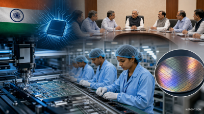
The Union Cabinet approved Semicon Mission 2.0 (outlay ₹1.27 lakh crore) and a new Mobile Phone Manufacturing Scheme (outlay ₹62,500 crore) on 15 July 2026, committing nearly ₹1.9 trillion to build domestic semiconductor capabilities and deepen mobile electronics value chains.
What is current and why it matters
Current policy action
- Two programmes: Semicon Mission 2.0 extends India’s semiconductor effort and the Mobile Phone Manufacturing Scheme replaces the earlier PLI-LSEM.
- Fiscal scale: Combined outlay is ₹1.895 lakh crore. Semicon Mission 2.0 targets ~₹4 lakh crore investment and ₹2 lakh crore production value; the mobile scheme targets ~₹39 lakh crore cumulative production and ~60,000 direct jobs.
- Operational signal: Three firms—Micron, Kaynes and CG Semi—are already operating commercial ATMP/OSAT lines under earlier measures. The first front-end fab under the programme (Tata-PSMC Dholera) is on a commissioning track (trial testing in late 2026; commercial scale-up by 2028).
Policy transition and structural change (ISM 1.0 → Semicon 2.0)
- Time-horizon: Policy lifecycle extended from 5 years to 12 years to provide long-term certainty for capital-intensive semiconductor projects.
- Six pillars: Design; equipment and materials manufacturing; fabs (front-end silicon fabrication); advanced packaging (ATMP/OSAT, HBM/ memory packaging); R&D; talent development.
- Strategic rebalancing: Shift from assembly-led outcomes to full-stack ecosystem building—emphasis on design/IP, domestic tooling and advanced packaging to capture higher value than mere final assembly.
Industrial strategy: mobile manufacturing and value addition
- Scheme design: Base incentives of 2.25–5% on eligible sales; bonus up to 1.5% for domestic component sourcing; 3% for design and R&D. Tenure: five years (FY2026‑27 to FY2030‑31).
- Policy objective: Encourage domestic brands, deeper local component supply chains, and onshore R&D rather than screwdriver assembly.
- Expected outcomes: Higher domestic value-add, export competitiveness, and concentrated manufacturing hubs with integrated component suppliers and test/pack facilities.
Infrastructure, resource and supply-chain challenges
- Capital intensity: Fabs require multi-billion-USD investments; private financing must be mobilised alongside fiscal incentives.
- Utilities: Fabs and advanced packaging need uninterrupted power, ultra-pure water and waste management at scale; these are local execution risks.
- Material and tooling dependence: Critical equipment (extreme ultraviolet lithography is not presently targeted but other specialised tools) and high-purity chemicals remain largely imported.
- Human capital: Shortage of specialised design, packaging and fab-operational talent; gap between academic output and industry skill profiles.
- Environmental and land clearances: Fabs require expedited but robust clearances for water and effluent management; regulatory delays raise project risk.
| Challenge | Policy/Operational response |
|---|---|
| High upfront cost | Longer policy horizon (12 years); fiscal incentives; blended public‑private financing and sovereign support for strategic fabs. |
| Utilities and logistics | Dedicated semiconductor parks with guaranteed water/power, pre‑cleared permissions and supply‑chain clustering. |
| Imported equipment/materials | Incentives for local equipment & materials manufacturing; technology partnerships for transfer and localisation. |
| Skill shortage | Industry‑aligned curricula, targeted skilling centres, fellowships and international training partnerships. |
Geopolitical and geoeconomic dimensions
- Supply‑chain resilience: Domestic capacity reduces vulnerability to concentrated production in East Asia and single‑supplier risks for strategic sectors.
- Technology diplomacy: Bilateral and plurilateral engagements (industry partnerships, iCET‑style cooperation, Japanese and US tie‑ups) secure technology transfer, investment and market access.
- Strategic autonomy: Onshore semiconductors support defence electronics, critical infrastructure and secure supply lines for telecom and aerospace.
- Friendly‑shoring: India can offer alternative manufacturing capacity to multinational firms seeking geographic diversification, conditional on regulatory predictability and logistics efficiency.
Institutional and financing measures
- Governance: A long policy window requires clear implementation architecture, single‑window clearances for semiconductor parks and predictable tariff/tax treatment.
- Financial instruments: Credit guarantees, concessional debt, viability gap funding for strategic fabs, and incentivised capex support for domestic tooling firms.
- Public‑private collaboration: Joint ventures (example: Tata‑PSMC) and risk‑sharing mechanisms to obtain advanced processes and market credibility.
Strategic way forward — priority actions
- Prioritise design and IP: Grants and tax breaks for chip design houses; support foundry‑agnostic design stacks.
- Build specialised parks: Integrated semiconductor precincts with assured utilities and logistics close to ports and component suppliers.
- Secure raw inputs: Technology diplomacy to access high‑purity chemicals, specialty gases and critical minerals.
- Localise tooling: Incentives for equipment manufacturers to set up in India and for global suppliers to establish service bases.
- Skilling pipeline: Centres of excellence in packaging, process control and VLSI design linked to industry apprenticeships.
- Export focus: Tie incentives to export commitments and global procurement linkages to ensure scale and market discipline.
Model Questions
1. Assess the strategic shift from India Semiconductor Mission 1.0 to Semicon Mission 2.0. How does a 12‑year policy horizon and the added focus on advanced packaging address structural vulnerabilities in India’s technology ecosystem? [GS-III: Science & Technology]
Semicon 2.0 extends policy certainty to 12 years, reducing investment risk for capital‑intensive fabs. It expands pillars to include design, equipment, materials and advanced packaging, moving value capture upstream from simple assembly. Advanced packaging and ATMP/OSAT strengthen memory and HBM capabilities, retain higher value domestically, and reduce dependence on foreign packaging. Long horizon supports financing, skills development and cluster creation needed for a full‑stack ecosystem.
2. Analyse how the new Mobile Phone Manufacturing Scheme incentivises domestic value addition and the emergence of Indian mobile brands compared with prior incentives. [GS-III: Economic Development]
The scheme provides 2.25–5% base incentives plus up to 1.5% for domestic component sourcing and 3% for design/R&D. This links rewards to local supply chains and IP creation rather than mere assembly. Tenure and export orientation aim to scale suppliers. The structure encourages vertical integration, local component industry growth and brand development, improving domestic value addition and export competitiveness.
3. Explain the geopolitical and economic implications of India building semiconductor fabrication and packaging capacity. What are the main resource and infrastructure constraints to be resolved? [GS-II: International Relations]
Domestic fabs reduce strategic dependence on concentrated foreign suppliers, improving supply‑chain resilience and defence preparedness. Economically, they cut import bills and enable industrial upgrading. Constraints include very high capital requirements, need for ultra‑pure water and stable power, reliance on imported specialised equipment and chemicals, limited skilled workforce, and regulatory/land‑clearance bottlenecks. Addressing these requires diplomacy, finance, and infrastructure planning.
4. Evaluate the role of international partnerships and technology diplomacy in India’s semiconductor strategy. What policy measures can ensure effective technology transfer and local capability building? [GS-III: Internal & External Security]
International partnerships provide capital, process know‑how and market links. Effective technology transfer needs clear IP arrangements, conditional incentives tied to localisation milestones, joint training programmes, and co‑investment structures. Policies should mandate local R&D centres, phased localisation targets, and facilitate industry‑academia exchange. Security vetting and export control alignment must balance openness with protection of critical technologies.
Last Modified: July 16, 2026