Rajasthan entered India’s semiconductor map with the virtual inauguration of its first semiconductor plant and an Electronics Manufacturing Cluster (EMC) at Salarpur, Khushkhera in Bhiwadi. Developed by the Electronic Industries Association of India (ELCINA) alongside Sahasra Semiconductors, the initiative aligns with the national Make in India, Digital India, and Atmanirbhar Bharat missions. The virtual opening followed an environment-focused approach to reduce fuel consumption. This expansion establishes the industrial belt near the Delhi-National Capital Region (NCR) as a high-technology production hub capable of generating employment and hosting microelectronics manufacturing units.
Infrastructure of the Bhiwadi Electronics Manufacturing Cluster
Area and Capital Allotment
The newly built Electronics Manufacturing Cluster covers an area of 50.3 acres. The project involved an investment of ₹46.09 crore, receiving a direct financial grant of ₹20.24 crore from the Central Government. The administrative layout provides utilities, including internal road systems, testing facilities, and dedicated resource connections.
Investment Profile and Job Creation
The cluster has drawn planned investments worth over ₹1,200 crore from approximately 20 domestic and international electronics enterprises. At present, 11 production units are operational within the hub with an active capital injection of ₹900 crore. These functional units have created more than 2,700 high-tech and manufacturing jobs.
Comprehensive Industrial Support
The complex features integrated administrative setups and an advanced Skill Development Centre equipped with smart classrooms and laboratories. The facilities handle diverse manufacturing segments, including semiconductor packaging, electronic components, Radio Frequency Identification (RFID) technologies, air-conditioners, Electric Vehicle (EV) components, and industrial electronics.
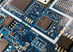
Sahasra Semiconductors ATMP and OSAT Unit
First SME-Led Semiconductor Facility
The unit established by Sahasra Semiconductors Pvt. Ltd. is India’s first Small and Medium Enterprise (SME) to achieve commercial production of semiconductor chips. Built under the Scheme for Promotion of Manufacturing of Electronic Components and Semiconductors (SPECS), the plant represents a capital investment of over ₹150 crore.
Plant Technical Specifications
The unit spans a floor area of 57,000 square feet and features specialized Class 10K and Class 100K industrial cleanrooms. These dust-controlled zones provide the environment required for Assembly, Testing, Marking, and Packaging (ATMP) along with Outsourced Semiconductor Assembly and Test (OSAT) procedures.
Product Range and Production Scaling
The plant produces integrated microelectronics and components, including:
- Memory chips for Micro SD cards and flash storage devices
- Light Emitting Diode (LED) driver Integrated Circuits (ICs)
- Embedded Subscriber Identity Modules (eSIMs)
- Radio Frequency Identification (RFID) tracking products
The manufacturing facility operates at a baseline capacity of 60 million semiconductor units per year. Plans seek to scale production volumes to 400–600 million units annually over the next two to three years.
Export Operations and Research Focus
The facility exports more than 60% of its total output to international markets, including the United States, France, Germany, Eastern Europe, China, and Nepal. Sahasra Semiconductors plans to expand operations into indigenous product Research and Development (R&D) to design domestic chip layouts and advanced LED driver components. It coordinates specialized technical training programs for local youth in partnership with the Electronics Sector Skills Council of India (ESSCI).
Strategic Profiles of Electronics and Semiconductor Hub Components
| Project Unit / Segment | Implementing Agency | Infrastructure Details | Primary Industrial Focus |
| Electronics Manufacturing Cluster (EMC) | ELCINA Electronics Manufacturing Cluster Pvt. Ltd. | 50.3 acres, ₹46.09 crore cost (₹20.24 crore central subsidy) | Electronic components, EV parts, and heavy appliances |
| Semiconductor ATMP/OSAT Facility | Sahasra Semiconductors Pvt. Ltd. | 57,000 sq. ft., Class 10K/100K cleanrooms, ₹150+ crore cost | Memory chips, eSIMs, and LED driver ICs |
| Technical Skilling Center | Joint tie-up with ESSCI & Technical Institutes | On-site smart classrooms and advanced laboratories | High-tech training and chip packaging skills |
The Rajasthan Semiconductor Policy 2026
Vision and Industrial Corridors
The State Government introduced the Rajasthan Semiconductor Policy 2026 to create a comprehensive chip ecosystem. The policy targets manufacturing growth in the Delhi-NCR linked industrial belt and sets up dedicated semiconductor corridors. These corridors include the Jodhpur-Pali-Marwar industrial region and the Kankani industrial area, both featuring fast-track clearances for land allocation and power linkage.
Financial and Fiscal Incentives
The state framework provides financial concessions to draw global and domestic chip developers:
- Electricity Benefits: 100% exemption from basic electricity duty for a period of seven years from operational launch.
- Land and Stamp Subsidies: A 75% rebate on standard stamp duty fees and mandatory land conversion charges.
- Capital Subsidies: Projects approved by the India Semiconductor Mission (ISM) receive up to a 60% supplementary state capital subsidy.
- Credit Benefits: Provision of a 5% interest subsidy on active commercial term loans.
Sustainability Frameworks
The policy mandates environmental criteria for semiconductor fabs and packaging units. Companies can claim up to a 50% reimbursement on specialized environmental management systems. It also includes full electricity duty waivers for factories transitioning to captive renewable energy sources.
IASPOINT Star Facts for UPSC
- ATMP vs. OSAT: Assembly, Testing, Marking, and Packaging (ATMP) refers to the physical backend processing of silicon wafers into finished chips. Outsourced Semiconductor Assembly and Test (OSAT) refers to independent third-party vendors performing these manufacturing services for fabless design firms.
- SPECS Scheme: The Scheme for Promotion of Manufacturing of Electronic Components and Semiconductors (SPECS) is managed by the Ministry of Electronics and Information Technology (MeitY). It offers a 25% financial incentive on capital expenditure for selected electronic goods and downstream semiconductor supply chains.
- Cleanroom Classifications: Class 10K (ISO 7) and Class 100K (ISO 8) cleanrooms denote strict particle limitation protocols. A Class 10K room permits a maximum of 10,000 particles (≥ 0.5 μ m) per cubic foot of air, which protects silicon layers from microscopic contamination.
- India Semiconductor Mission (ISM): Launched as a specialized business division within the Digital India Corporation, ISM drives India’s ₹76,000 crore semiconductor ecosystem program. It oversees financial evaluations for silicon fabs, display production plants, and ATMP facilities.
- Fabless Semiconductor Model: This industrial system splits chip production into two distinct corporate entities. Fabless firms handle the initial software layout, micro-architecture, and hardware design, while outsourcing the hardware fabrication to dedicated external foundries or OSAT centers.